

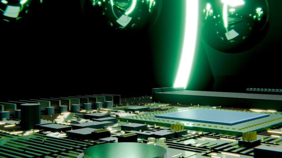
Alright, let’s dive into how optical computing is stepping up to supercharge Large Language Model (LLM) training, especially in those massive hyperscale data centers we’re seeing pop up everywhere. The short answer is that optical computing promises to dramatically boost the speed and energy efficiency of LLM training by moving beyond traditional electronic limitations, offering a completely different way to process information, particularly the matrix multiplications that are the bread and butter of neural networks.
The Looming Challenge for LLMs
Training these behemoth LLMs, like GPT-3 or even larger models, has become an absolutely monumental task. We’re talking about billions, sometimes trillions, of parameters that need to be updated across vast datasets. This process is inherently compute-intensive and, crucially, data-intensive.
The Data Avalanche
Every new iteration of an LLM seems to demand even more data. This isn’t just about the sheer volume of text; it’s also about the increasing complexity and diversity of that data. Handling terabytes upon terabytes of training data efficiently is a huge bottleneck.
The Compute Crunch
Modern GPUs have been incredible workhorses for AI, but even they are starting to hit limits. The fundamental architecture of electronic computing – moving electrons, generating heat, and dealing with signal integrity over copper wires – creates bottlenecks that become exponentially more problematic as models scale.
Energy Demands and Environmental Impact
The energy consumed by training a single large LLM can be staggering, sometimes equivalent to several households’ annual consumption. As we push for more frequent retraining and even larger models, the environmental footprint and operational cost become unsustainable without fundamental changes. Optical computing offers a path toward significantly lower power consumption per operation.
In the rapidly evolving landscape of technology, the intersection of optical computing and artificial intelligence is gaining significant attention, particularly in the context of large language model training in hyper-scale datacenters. A related article that explores the broader implications of technology in social media can be found at Instagram Adds a Dedicated Spot for Your Pronouns. This piece highlights how advancements in digital platforms are adapting to user needs, paralleling the way optical computing is set to revolutionize data processing and model training efficiency.
Why Traditional Electronics Are Hitting the Wall
To understand why optics is so exciting, we first need to quickly grasp the limitations of our current electronic setup. It’s not that electronics are bad; they’re just not ideal for everything, especially the specific computational patterns of deep learning.
The von Neumann Bottleneck
Our conventional computers operate on the von Neumann architecture, which separates the processing unit from memory. This means data constantly shuttles back and forth between the CPU/GPU and RAM. For LLMs, where massive amounts of data are being accessed and processed repeatedly, this data movement becomes a major slowdown and energy drain. It’s like having a chef constantly running to a different building for each ingredient.
Interconnect Limitations
Inside a data center, and even within a single chip, data moves over electrical interconnects – copper wires. These wires have resistance, which leads to signal degradation, latency, and heat generation. As speeds increase, these issues worsen, requiring more power to drive signals and more complex cooling solutions. This becomes particularly problematic for the massive parallel communication required for distributed LLM training.
Power and Heat Dissipation
Every time electrons move, they generate heat. The denser the circuitry and the faster the clock speeds, the more heat is produced. This necessitates elaborate and energy-hungry cooling systems. For hyperscale data centers, managing this heat is a significant operational challenge and cost factor. Optical computing, by contrast, uses photons, which don’t have mass or charge, and thus generate far less heat during data transmission.
The Promise of Optical Computing
Optical computing, at its core, uses photons (light) instead of electrons to perform calculations and transmit information. This fundamental shift opens up a world of possibilities that electronic systems simply can’t match for certain types of tasks.
Speed of Light Transmission
This might seem obvious, but photons travel at the speed of light. While electrons also move fast, they’re constrained by resistance and capacitance in wires. Optical signals, particularly within waveguides or fiber optics, can carry information over longer distances with virtually no latency or signal degradation, making them ideal for high-speed, long-distance communication within a data center or even across chips.
Parallelism Through Wavelength Division Multiplexing (WDM)
One of the coolest tricks optics offers is Wavelength Division Multiplexing (WDM). Imagine sending multiple separate data streams down a single optical fiber, each stream using a different color (wavelength) of light. It’s like having many separate lanes on a highway, all traveling at the same speed, but completely independent. This allows for massive parallel data transmission and processing, which is incredibly valuable for the highly parallel nature of neural network operations.
Analog Computation for Matrix Multiplications
Here’s where optical computing really shines for LLMs. The core of neural network operations, especially in LLMs, is matrix multiplication (e.g., weights multiplied by inputs). Electronic systems perform these as a series of discrete, digital operations. Optical systems, however, can perform matrix multiplications in an analog fashion. Light waves can interfere constructively or destructively, and this interference can directly represent the summation and multiplication required. This means an entire matrix multiplication can happen almost instantaneously at the speed of light, rather than step-by-step.
Reduced Power Consumption
Because photons don’t generate heat in the same way electrons do, optical computation and transmission promise significantly lower power consumption, especially for highly parallel operations. This translates directly to lower operating costs and a smaller environmental footprint for hyperscale data centers.
How Optical Computing Accelerates LLM Training
Now let’s get specific about how these optical advantages translate into real-world benefits for LLM training. It’s about tackling the bottlenecks we discussed earlier head-on.
In-Memory Computing Architectures
One of the most promising applications is integrating optical components directly into or very close to memory. This allows for a form of “in-memory computing” where computations happen right where the data resides, drastically reducing the need to move data back and forth between separate processing and memory units.
Optical RAM (ORAM) Concepts
While still in early research, the idea of truly optical RAM, where data is stored and retrieved optically, holds immense potential. This would eliminate the electronic-to-optical conversion overhead that current hybrid systems still face.
Photonic Integrated Circuits (PICs) for Processing
Photonic Integrated Circuits (PICs) are like microchips but for light. They can integrate optical waveguides, modulators, and detectors onto a single chip. These PICs can be designed specifically to accelerate matrix multiplications, acting as dedicated optical linear algebra units that bypass the electronic bottleneck for these critical operations.
Accelerating Matrix Multiplication with Light
As mentioned, the analog nature of optical computation makes it supremely efficient for matrix multiplication, the foundational operation of neural networks.
Optical Linear Algebra Units
These dedicated optical processors can perform hundreds or thousands of multiply-accumulate (MAC) operations simultaneously using interference patterns. Instead of billions of discrete transistor operations, it’s a single physical phenomenon. This translates to orders of magnitude faster computation for these specific operations.
Benefits for Attention Mechanisms
The “attention” mechanism, a cornerstone of transformer architectures used in LLMs, heavily relies on large-scale matrix multiplications. By speeding up these operations optically, the computational cost of attention can be drastically reduced, allowing for larger context windows and more complex attention patterns without incurring prohibitive latency.
High-Bandwidth, Low-Latency Interconnects
Even if the processing itself is happening on optical chips, the data still needs to get to and from these chips and between different computational units within the data center.
Fiber Optic Backbones for Data Centers
Hyperscale data centers are already heavy users of fiber optics for their backbone networks. Optical computing extends this principle to within the racks and even between chips, further reducing latency and increasing bandwidth.
On-Chip Optical Interconnects
Imagine replacing the tiny copper wires connecting different modules on a single chip with optical waveguides. This would eliminate many of the power and heat issues associated with electrical interconnects at the incredibly fine scales required for modern processors. This is sometimes referred to as “photonic fabric.”
In exploring the advancements in computing technologies, a fascinating article discusses the implications of optical computing on large language model training in hyper-scale datacenters. This innovative approach not only enhances processing speeds but also significantly reduces energy consumption, making it a game-changer for AI development. For those interested in optimizing their tech choices, understanding how to select the right devices is crucial, as highlighted in this informative piece on choosing laptops for students. By staying informed about these technological trends, one can better appreciate the evolving landscape of computing.
Challenges and the Road Ahead
While the promise is huge, optical computing for LLMs isn’t without its hurdles. It’s a complex field, and there’s still a lot of R&D happening.
Integration with Existing Electronic Systems
We’re not going to throw away all our electronic chips overnight. The most realistic path forward involves hybrid systems that combine the strengths of both. This means developing efficient and low-loss optical-to-electrical and electrical-to-optical converters (O/E and E/O). These conversions are currently a significant challenge.
Hybrid Opto-Electronic Architectures
The first commercial products will almost certainly be hybrid, with optical components acting as accelerators or specialized modules alongside traditional electronic processors. The design of these hybrid architectures needs to optimize the workflow to minimize conversion overheads.
Software and Compiler Adaptations
Current AI frameworks (like TensorFlow or PyTorch) and compilers are heavily optimized for electronic architectures. To fully leverage optical hardware, new software layers, compilers, and programming paradigms will need to be developed that can effectively map LLM computations onto these novel optical systems. This is a non-trivial undertaking.
Manufacturing and Scaling
Producing high-performance, reliable photonic integrated circuits at scale is a significant engineering challenge. The materials, fabrication processes, and testing methodologies are different from those for silicon electronics and are still maturing.
Material Science for Photonic Devices
Developing new materials with optimal optical properties, low loss, and compatibility with existing semiconductor manufacturing processes is an active area of research. Silicon photonics is a promising avenue here because it leverages existing silicon manufacturing infrastructure.
Yield and Cost of Optical Components
Initially, the yield for complex optical integrated circuits might be lower, leading to higher costs. As manufacturing processes mature and demand increases, we can expect costs to come down, but it will take time for optical components to reach cost parity with highly mature electronic components.
Precision and Noise in Analog Computation
The analog nature of optical computation, while powerful for speed, introduces challenges related to precision and noise. Electronic digital systems offer very high precision (e.g., 32-bit or 64-bit floating-point numbers). Optical analog systems need careful design to maintain sufficient precision for LLM training, where small errors can accumulate.
Error Correction and Mitigation Strategies
Researchers are exploring various techniques to mitigate noise and maintain precision in optical analog computations, including advanced calibration methods and novel architectural designs that can tolerate some level of analog imprecision. This is crucial for the convergence of training algorithms.
Balancing Analog Speed with Digital Accuracy
The key will likely be finding the right balance: using analog optical computation for the “heavy lifting” of matrix multiplications where some imprecision is tolerable, and relying on digital electronics for other parts of the LLM pipeline that require high precision or complex control logic.
In closing, optical computing isn’t a silver bullet that will immediately replace all electronic computation.
Instead, it’s a powerful new tool in the arsenal for tackling the escalating demands of AI, especially for LLMs in hyperscale data centers.
By leveraging the fundamental properties of light, it promises a future where LLMs can be trained faster, more efficiently, and with a significantly smaller energy footprint, ultimately unlocking even more complex and capable AI models. The transition will be gradual, involving hybrid systems and new approaches to software, but the direction is clear: light will play an increasingly vital role in powering the AI revolution.
FAQs
What is optical computing?
Optical computing is a computing technology that uses photons to perform operations on data. It has the potential to significantly accelerate processing speeds and reduce energy consumption compared to traditional electronic computing.
How does optical computing accelerate large language model training in hyper-scale datacenters?
Optical computing accelerates large language model training in hyper-scale datacenters by leveraging the speed of light to perform computations. This allows for faster processing of large amounts of data, which is essential for training complex language models.
What are the benefits of using optical computing in hyper-scale datacenters?
The benefits of using optical computing in hyper-scale datacenters include faster processing speeds, reduced energy consumption, and the ability to handle large amounts of data more efficiently. This can lead to significant cost savings and improved performance for language model training and other data-intensive tasks.
Are there any challenges or limitations associated with optical computing in hyper-scale datacenters?
While optical computing offers many advantages, there are also challenges and limitations to consider. These may include the cost of implementing optical computing infrastructure, the need for specialized hardware and software, and potential compatibility issues with existing systems.
What is the potential impact of optical computing on the future of large language model training in hyper-scale datacenters?
The potential impact of optical computing on the future of large language model training in hyper-scale datacenters is significant. It has the potential to revolutionize the way data is processed and analyzed, leading to faster and more efficient training of language models and other data-intensive tasks.
Enjoying our content? Make us a preferred source on Google:
Add us as a Preferred Source on Google