

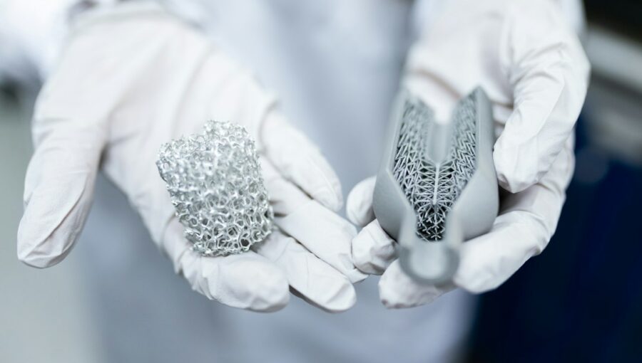
So, what’s the deal with biodegradable substrates and eco-friendly polymers in modern semiconductor manufacturing? Basically, it’s about making computer chips with materials that are better for the planet, moving away from traditional, often toxic, and non-biodegradable options. We’re talking about finding ways to produce the incredibly complex components that power our devices without leaving a massive environmental footprint behind. This isn’t just some niche scientific curiosity; it’s a growing area of research and development that aims to address the significant waste and pollution generated by the electronics industry.
The Environmental Imperative for Greener Electronics
The electronics industry is a powerhouse of innovation, but it also has a significant environmental shadow. From resource extraction for raw materials to energy-intensive manufacturing processes and the ever-growing problem of electronic waste (e-waste), the lifecycle of our devices is far from sustainable. This isn’t a new problem, but it’s one that’s becoming increasingly urgent as our reliance on electronics continues to grow exponentially.
The Problem with Traditional Materials
Current semiconductor manufacturing relies heavily on materials like silicon, gallium arsenide, and various plastics and epoxies for encapsulation. While these materials have enabled incredible technological advancements, many of them are problematic. Silicon production is energy-intensive, and the etching and cleaning processes often involve hazardous chemicals. The plastics used in packaging and circuit boards are typically petroleum-derived, non-biodegradable, and contribute significantly to landfill waste. Heavy metals like lead, mercury, and cadmium, though increasingly phased out, still linger in older devices and pose risks during disposal. The sheer volume of e-waste generated globally is staggering, often ending up in landfills where toxic substances can leach into the soil and groundwater, or being informally recycled in ways that expose workers and communities to dangerous chemicals.
The Push Towards Sustainability
Recognizing these challenges, there’s a strong push within the industry, driven by both regulatory pressures and consumer demand, to develop more sustainable manufacturing practices. This includes everything from optimizing energy consumption in factories and reducing water usage to exploring closed-loop recycling systems. However, a fundamental shift involves rethinking the materials themselves. This is where biodegradable substrates and eco-friendly polymers come into play. The idea is to create components that, at the end of their useful life, can either safely break down into benign substances or be easily recycled, minimizing their long-term environmental impact. This isn’t just about feeling good; it’s about future-proofing an industry that’s critical to modern life.
In the realm of sustainable technology, the exploration of biodegradable substrates and eco-friendly polymers in modern semiconductor manufacturing is gaining significant attention. These innovations not only aim to reduce environmental impact but also enhance the efficiency of electronic devices. For those interested in the intersection of technology and sustainability, a related article discussing the best free drawing software for digital artists can provide insights into how creative tools are evolving alongside these advancements. You can read more about it here: Best Free Drawing Software for Digital Artists in 2023.
Key Takeaways
- The training data includes information and events up to October 2023.
- Insights and knowledge are based on a wide range of sources available until the cutoff date.
- No updates or developments occurring after October 2023 are included in the training.
- Users should verify current information from reliable sources for the latest updates.
- The model’s responses reflect the context and knowledge available up to the specified date.
Biodegradable Substrates: A Foundation for Change

Substrates are the foundational layers upon which semiconductor circuits are built. Traditionally, these are rigid, non-biodegradable materials like silicon wafers or ceramic. The move towards biodegradable substrates represents a radical rethinking, aiming to create circuit boards and chip foundations that can naturally decompose after use.
Natural Polymer-Based Substrates
One promising avenue involves using natural polymers derived from renewable resources. These materials offer the advantage of being inherently biodegradable, reducing the environmental burden of disposal.
Cellulose and Paper-Based Substrates
Cellulose, the primary component of plant cell walls, is abundant, renewable, and naturally biodegradable. Paper, essentially processed cellulose, has been explored as a substrate material. Researchers are developing methods to treat paper to make it more suitable for electronic applications, including improving its smoothness, electrical insulation properties, and resistance to moisture. While paper substrates are still primarily in the research phase for high-performance applications, they show great promise for low-cost, disposable, and flexible electronics, such as smart labels, sensors, or even some medical patches. Challenges include achieving sufficient dimensional stability, surface roughness, and thermal resistance for conventional semiconductor processing.
Starch and Chitin-Based Substrates
Starch, another abundant natural polymer found in plants, is also being investigated. Starch-based bioplastics can be processed into films that could potentially serve as flexible substrates. Similarly, chitin, found in the exoskeletons of insects and crustaceans, is a highly promising material. It’s biodegradable, biocompatible, and can be processed into flexible films with good mechanical properties. Chitin and its derivative, chitosan, have shown potential for applications in transient electronics – devices designed to dissolve or degrade after a specific function or time, which is incredibly useful for things like temporary medical implants or environmental sensors. The key here is engineering these natural materials to meet the stringent requirements of semiconductor fabrication, which often involves high temperatures and harsh chemical environments.
Protein and Silk-Based Substrates
Proteins offer another class of biodegradable materials with unique properties. Silk fibroin, derived from silkworms, is particularly interesting due to its excellent mechanical strength, flexibility, biocompatibility, and optical transparency. Silk can be processed into thin films or fibers that serve as robust, yet degradable, substrates. It’s been explored for implantable biomedical devices and transient electronics where biocompatibility and controlled degradation are crucial. The ability to precisely control silk’s degradation rate by varying its crystalline structure makes it highly versatile. However, integrating silk processing with standard semiconductor fabrication techniques still requires significant research and development. The cost and scalability of silk production also need to be considered for widespread adoption.
Engineering Challenges for Biodegradable Substrates
While natural materials offer clear environmental benefits, adapting them for semiconductor manufacturing presents several hurdles.
Thermal Stability and Chemical Resistance
Traditional semiconductor processes often involve high temperatures (e.g., for annealing or deposition) and exposure to harsh chemicals (e.g., strong acids or solvents for etching and cleaning). Many natural polymers are not inherently stable under these conditions, leading to degradation, deformation, or chemical reactions that compromise device performance. Research focuses on modifying these materials, or developing new low-temperature processing techniques compatible with them. This might involve surface treatments, cross-linking, or blending with other more resilient polymers.
Electrical and Mechanical Properties
The electrical properties of a substrate are critical – it needs to be a good insulator to prevent signal leakage and crosstalk. Natural materials can sometimes have higher dielectric losses or absorb more moisture, which affects their electrical performance. Mechanically, a substrate needs to be strong enough to withstand handling during manufacturing and flexible enough for certain applications, while also maintaining dimensional stability. Achieving the right balance of these properties in biodegradable materials, which can vary greatly in their natural state, is a complex engineering task. For example, ensuring a paper substrate remains flat and doesn’t warp during processing is a significant challenge.
Surface Roughness and Interfacial Adhesion
Semiconductor devices feature incredibly small structures, often at the nanometer scale. This demands extremely smooth substrate surfaces to ensure uniform film deposition and proper device operation. Natural materials often have inherent surface roughness or inhomogeneities that need to be overcome. Furthermore, achieving strong adhesion between the substrate and subsequent deposited layers (like metal interconnects or active semiconductor films) is crucial for device reliability. Poor adhesion can lead to delamination and device failure, especially in flexible or transient applications. Surface modification techniques, such as plasma treatment or chemical functionalization, are being explored to address these issues.
Eco-Friendly Polymers in Device Encapsulation and Interconnects
Beyond the substrate, polymers play a crucial role in modern semiconductors, primarily for encapsulation (protecting the chip) and as dielectric layers in interconnects (insulating wiring). Shifting these applications to eco-friendly polymers can significantly reduce the overall environmental impact.
Biodegradable Encapsulants
Encapsulation is vital for protecting delicate semiconductor dies from moisture, contaminants, and mechanical stress. Traditionally, epoxy resins, which are non-biodegradable, are used.
Developing biodegradable alternatives is a major focus.
Polylactic Acid (PLA) and Polyhydroxyalkanoates (PHAs)
PLA is a well-known biodegradable polyester derived from renewable resources like corn starch or sugarcane. It has good mechanical properties and can be processed using standard techniques like injection molding. While PLA has found widespread use in packaging and biomedical applications, its application in semiconductor encapsulation requires careful consideration of its thermal stability and moisture permeability.
Researchers are modifying PLA to improve these properties, often by blending it with other polymers or incorporating fillers. PHAs are another family of biodegradable polyesters produced by microorganisms. They offer a wider range of properties, from rigid to flexible, and are generally more biodegradable than PLA in various environments.
Their tunable properties make them attractive for encapsulation, but their higher cost and more complex processing can be barriers to widespread adoption.
Other Bio-Based and Degradable Polymers
Beyond PLA and PHAs, a variety of other bio-based and degradable polymers are being explored. These include aliphatic polyesters (like polycaprolactone, PCL), protein-based polymers, and even natural rubber derivatives. The key is to find materials that not only biodegrade but also meet the stringent performance requirements for encapsulation: low moisture absorption, good adhesion to the chip, thermal stability during operation, and mechanical robustness.
Some research is also looking into dynamically degradable polymers, which can be triggered to degrade under specific environmental conditions (e.g., pH change, light exposure), offering more controlled disposal options.
Green Dielectrics and Interlayer Materials
Dielectric layers insulate different parts of a chip, preventing short circuits and signal interference. In advanced semiconductor nodes, low-k dielectrics (materials with low dielectric constant) are crucial for faster signal propagation. Many traditional low-k materials contain fluorine or other elements that can be environmentally persistent.
Cellulose Nanofibers and Nanocrystals
Cellulose, particularly in its nanofiber (CNF) or nanocrystal (CNC) forms, offers exciting possibilities for green dielectrics.
These materials have excellent electrical insulation properties, high mechanical strength, and are naturally biodegradable. They can be processed into thin films with good optical transparency and low dielectric constant, making them suitable for interlayer dielectrics or even as components in flexible display technologies. The challenge lies in uniformly dispersing these nanoparticles within a polymer matrix to achieve homogeneous films and integrating them into existing semiconductor fabrication lines without introducing defects.
Bio-Based Epoxy Resins
While traditional epoxy resins are problematic, research is progressing on developing bio-based alternatives.
These new epoxy resins are synthesized using precursors derived from renewable biomass sources (e.g., vegetable oils, lignin) rather than petroleum. The goal is to create epoxies with comparable or even superior thermal and mechanical properties to their petroleum-based counterparts, but with a reduced carbon footprint and potentially improved degradability profiles. While they might not be fully biodegradable in the same way as PLA, they represent a step towards more sustainable materials in the epoxy family, which are critical for many semiconductor applications.
Challenges in Polymer Integration
Integrating these new polymers into existing manufacturing flows is not straightforward.
Process Compatibility
Semiconductor manufacturing is a highly optimized, multi-step process.
New materials must be compatible with existing equipment, temperatures, pressures, and chemical environments. For instance, processes like chemical vapor deposition (CVD) or atomic layer deposition (ALD) often operate at high temperatures, which might degrade bio-based polymers. Developing new low-temperature deposition techniques or modifying the polymer structure to withstand higher temperatures are active areas of research.
Compatibility with etching processes, photolithography, and cleaning steps is also critical.
Performance Durability and Reliability
Electronics need to be reliable over their intended lifespan, often many years. Eco-friendly polymers must demonstrate comparable or superior durability, thermal stability, moisture resistance, and mechanical integrity to traditional materials. This is particularly challenging for biodegradable materials, which by definition are designed to break down.
Balancing the need for performance during operation with degradability at end-of-life is a key design consideration. Accelerated aging tests and rigorous reliability assessments are essential to ensure these new materials can meet industry standards.
Cost and Scalability
Many bio-based polymers and specialized biodegradable materials are currently more expensive than their traditional counterparts, primarily due to smaller production volumes and less mature supply chains. For widespread adoption, the cost needs to be competitive.
Scalability of production is also a concern; can these materials be produced in the massive quantities required by the semiconductor industry without significant environmental or economic drawbacks? This requires investment in infrastructure and process optimization for large-scale manufacturing of these greener alternatives.
Emerging Technologies and Future Prospects
The field of sustainable semiconductor manufacturing is rapidly evolving, with several exciting technologies pushing the boundaries of what’s possible.
Transient Electronics and Bio-Resorbable Devices
Transient electronics are devices designed to perform a specific function for a defined period and then completely disappear or degrade harmlessly into the environment or within a biological system. This concept is revolutionary, particularly for medical implants, environmental sensors, and secure data storage.
Materials for Controlled Degradation
The key to transient electronics lies in materials with precisely controllable degradation rates. Besides silk and some PHAs, researchers are exploring magnesium and zinc alloys for biodegradable metallic conductors, and various natural waxes or polymers for encapsulation that can be triggered to dissolve by specific solvents, pH changes, or temperature fluctuations. The goal is to design devices where every component—substrate, conductor, dielectric, and active semiconductor—can degrade on demand. This requires a deep understanding of material science and degradation mechanisms, ensuring that the byproducts of degradation are non-toxic.
Applications in Medicine and Environmental Monitoring
In medicine, bio-resorbable electronic implants could monitor vital signs or deliver drugs, then dissolve away, eliminating the need for removal surgery. This reduces patient risk and healthcare costs. Examples include temporary pacemakers, nerve regeneration scaffolds, or smart wound dressings. For environmental monitoring, transient sensors could be deployed to track pollutants or soil conditions and then degrade without leaving behind electronic waste.
This has vast implications for smart agriculture and remote sensing in sensitive ecosystems.
The ability to “program” the lifetime of an electronic device opens up entirely new paradigms for interaction with the physical world.
Hybrid Approaches and Material Blends
Purely biodegradable devices for all applications are still a long way off, especially for high-performance computing. Hybrid approaches, combining traditional and eco-friendly materials, often offer a more pragmatic near-term solution.
Combining Biodegradable and Non-Biodegradable Components
This involves using biodegradable substrates or encapsulants in conjunction with traditional silicon chips or metallic interconnects. For instance, a silicon chip could be mounted on a paper-based substrate and then encapsulated with a PLA-based polymer. While the silicon chip itself isn’t biodegradable, the bulk of the supporting materials are, significantly reducing the e-waste footprint. This approach allows for a phased transition, gradually incorporating more sustainable materials without requiring a complete overhaul of core semiconductor technology. It leverages the strengths of existing high-performance components while mitigating the environmental impact of their packaging and support structures.
Blending for Enhanced Properties
Material blending is another powerful technique. By combining a biodegradable polymer with small amounts of non-biodegradable but high-performance additives (e.g., ceramic nanoparticles, carbon nanotubes), engineers can create composites that retain much of the biodegradability while enhancing properties like thermal conductivity, mechanical strength, or electrical insulation. For example, a cellulose composite might be developed by incorporating silicon dioxide nanoparticles to improve its rigidity and moisture barrier properties. This allows for fine-tuning of material characteristics to meet specific application requirements, providing a bridge between ideal biodegradability and necessary performance. The challenge lies in ensuring that the additives do not hinder the overall degradation process or introduce new toxic components.
Recycling and End-of-Life Management Innovations
Even with biodegradable materials, effective end-of-life management is crucial. Not all electronics will biodegrade perfectly in every environment, and some will still contain valuable metals or components that should be recovered.
Design for Disassembly
Designing electronics with disassembly in mind is key to efficient recycling. This means using fewer different materials, avoiding permanent bonding agents where possible, and clearly labeling components. For example, using snap-fit enclosures instead of glued ones, or choosing adhesives that can be easily dissolved. This makes it easier to separate different material streams (metals, plastics, glass) for recycling or composting. When components can be easily separated, valuable resources can be recovered more effectively, reducing the need for virgin materials and minimizing waste.
Novel Recycling Processes for Bio-Based Materials
Traditional recycling infrastructure is not yet equipped to handle bio-based or biodegradable electronics. New processes are needed to either compost these materials effectively or to chemically recycle them back into their monomers for reuse. Chemical recycling, which breaks down polymers into their constituent building blocks, holds significant promise for creating a circular economy for plastics. For biodegradable materials, industrial composting facilities will need to be developed or adapted to handle these types of e-waste, ensuring they break down completely and safely. This requires a concerted effort from manufacturers, waste management companies, and policymakers to establish the necessary infrastructure and standards.
In the realm of sustainable technology, the exploration of biodegradable substrates and eco-friendly polymers in modern semiconductor manufacturing is gaining significant attention. A related article discusses the innovative features of the Samsung Galaxy Chromebook 4, which showcases how advancements in technology can align with environmental consciousness. This intersection of eco-friendly materials and cutting-edge devices highlights the potential for a greener future in electronics. For more insights, you can read the article here.
The Road Ahead: Challenges and Opportunities
| Metric | Description | Value / Range | Unit | Notes |
|---|---|---|---|---|
| Biodegradability Rate | Time taken for substrate/polymer to degrade under composting conditions | 3-12 | Months | Depends on material composition and environmental conditions |
| Thermal Stability | Maximum temperature substrate/polymer can withstand without degradation | 150-300 | °C | Critical for semiconductor processing steps |
| Dielectric Constant (k) | Measure of insulating properties of polymer | 2.0-3.5 | Unitless | Lower k-values reduce parasitic capacitance |
| Mechanical Strength | Tensile strength of biodegradable substrate/polymer | 30-80 | MPa | Ensures durability during manufacturing |
| Environmental Impact Score | Relative environmental footprint compared to conventional materials | 0.3-0.7 | Index (0-1) | Lower values indicate better eco-friendliness |
| Electrical Conductivity | Conductivity of polymer when doped or modified | 10-12 – 10-8 | S/m | Typically insulating but can be tailored |
| Water Absorption | Percentage of water absorbed by substrate/polymer | 0.1-2.0 | % | Lower absorption preferred for stability |
| Processing Compatibility | Compatibility with standard semiconductor fabrication processes | High / Medium / Low | Qualitative | Depends on polymer chemistry and substrate design |
While the vision of truly sustainable semiconductor manufacturing is compelling, getting there involves significant challenges and presents numerous opportunities for innovation.
Overcoming Technical Hurdles
As discussed, achieving thermal stability, chemical resistance, precise electrical properties, and mechanical robustness in biodegradable materials, all while maintaining cost-effectiveness and scalability, is a monumental task. The complexity of integrating these new materials into existing, highly specialized fabrication processes cannot be underestimated.
This requires deep collaboration between material scientists, electrical engineers, and process engineers.
Research into novel synthesis methods, surface modifications, and advanced composite materials will be critical. Developing new manufacturing equipment and techniques specifically tailored for these greener materials might also be necessary, representing a substantial investment.
Regulatory and Economic Considerations
For widespread adoption, regulatory frameworks will need to evolve to incentivize the use of sustainable materials and properly manage end-of-life options. This includes establishing clear standards for biodegradability and compostability, as well as developing policies that support the development of recycling infrastructure for these new material streams. Economically, the cost of sustainable materials and processes needs to become competitive with traditional methods. Government subsidies, research grants, and consumer demand can help drive down costs and accelerate adoption. Companies also need to see a clear business case, whether through reduced waste disposal costs, enhanced brand image, or compliance with upcoming environmental regulations.
Industry Collaboration and Standardization
No single company or research institution can tackle this challenge alone. Widespread industry collaboration is essential, sharing knowledge, best practices, and even pooling resources for fundamental research. Developing common standards for materials, testing protocols, and manufacturing processes will be crucial to ensure interoperability and to build confidence in these new technologies. This includes working with international bodies to create global standards that facilitate the adoption of sustainable electronics across borders. A unified approach will accelerate progress and avoid fragmented efforts.
Consumer Awareness and Acceptance
Ultimately, the success of greener electronics depends on consumer acceptance. Educating consumers about the benefits of these devices – from reduced environmental impact to potential new functionalities (like transient medical devices) – is vital. As consumers become more aware of the environmental footprint of their electronics, their demand for sustainable alternatives will grow, further driving industry innovation. This includes clear labeling and communication about the biodegradability or recyclability of products, helping consumers make informed choices and participate in proper end-of-life disposal.
The shift towards biodegradable substrates and eco-friendly polymers in semiconductor manufacturing is not just an incremental improvement; it represents a fundamental paradigm shift. It’s about building a future where our technological advancements don’t come at the cost of our planet. While the challenges are considerable, the opportunities for innovation, environmental stewardship, and new product development are even greater. This isn’t just about making chips, it’s about making a difference.
FAQs
What are biodegradable substrates in semiconductor manufacturing?
Biodegradable substrates are materials used as a base for semiconductor manufacturing that can naturally decompose or break down into harmless compounds over time, reducing environmental impact.
How do biodegradable substrates contribute to eco-friendly semiconductor manufacturing?
Biodegradable substrates help reduce the use of traditional non-biodegradable materials in semiconductor manufacturing, leading to a more sustainable and environmentally friendly process.
What are eco-friendly polymers and their role in modern semiconductor manufacturing?
Eco-friendly polymers are sustainable materials that can be used in place of traditional polymers to reduce the environmental footprint of semiconductor manufacturing processes, contributing to a greener industry.
What are the benefits of using biodegradable substrates and eco-friendly polymers in semiconductor manufacturing?
The use of biodegradable substrates and eco-friendly polymers can help lower carbon emissions, reduce waste generation, and promote a more sustainable approach to semiconductor production, benefiting both the industry and the environment.
Are there any challenges or limitations associated with the adoption of biodegradable substrates and eco-friendly polymers in semiconductor manufacturing?
While biodegradable substrates and eco-friendly polymers offer environmental benefits, challenges such as cost, performance, and scalability need to be addressed to ensure widespread adoption in modern semiconductor manufacturing processes.
Enjoying our content? Make us a preferred source on Google:
Add us as a Preferred Source on Google