

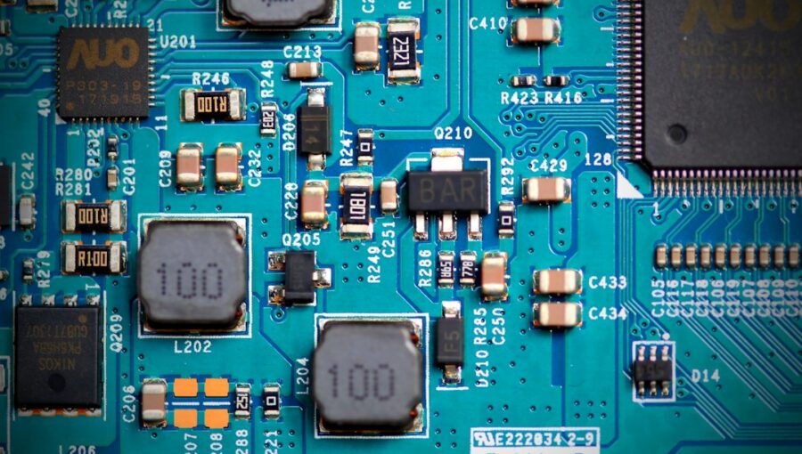
So, can we really have Printed Circuit Boards (PCBs) that just disappear into nature when we’re done with them? The short answer is yes, we can – and there’s a lot of exciting work happening in biodegradable PCBs. It’s not a magic bullet yet, and there are definitely some hurdles to overcome before they become mainstream, but the viability is there, and the performance is getting better all the time. The biggest challenges currently revolve around manufacturing at scale and ensuring consistent performance over a product’s intended lifespan.
The Growing Need for Eco-Friendly Electronics
We’re all pretty reliant on electronics these days, from our smartphones to smart home gadgets. The problem is, once these devices reach their end-of-life, they often become electronic waste, or e-waste. This stuff is a real headache for the environment because it contains a mix of materials, some of which are toxic and don’t break down naturally. Landfills are piling up with old circuit boards, and the recycling processes aren’t always perfect or cost-effective for every component.
The Environmental Burden of Conventional PCBs
Standard PCBs are typically made from fiberglass (FR-4) reinforced with epoxy resin, copper traces, and various solders and coatings. While incredibly durable and reliable, these materials are designed to last, which is great for a device’s lifetime but terrible for disposal. When these boards end up in landfills or are improperly incinerated, they can release heavy metals like lead and cadmium, brominated flame retardants (BFRs), and other persistent organic pollutants into the soil, water, and air. This not only harms wildlife and ecosystems but can also pose significant health risks to humans. The sheer volume of e-waste is staggering and continues to grow as technology advances and product lifecycles shorten. Finding alternatives that reduce this environmental impact is becoming increasingly urgent.
Why “Biodegradable” is More Than Just a Buzzword
When we talk about “biodegradable,” we’re aiming for materials that can break down into natural components – think water, carbon dioxide, and biomass – through biological processes, usually with the help of microorganisms. For PCBs, this means the entire board, or at least its key structural and conductive components, would eventually decompose without leaving behind harmful residues. This isn’t just about reducing landfill waste; it’s also about conserving valuable resources. Manufacturing conventional PCBs requires significant energy and often involves hazardous chemicals. Biodegradable alternatives offer a path toward a more circular economy where materials can return to nature, reducing the demand for virgin resources and lessening the environmental footprint from cradle to grave. It’s a holistic approach to sustainability in electronics.
In exploring the advancements in sustainable technology, the article on biodegradable printed circuit boards highlights not only their viability and performance but also the significant manufacturing challenges they face. For a broader perspective on how these innovations align with current trends, you may find it insightful to read about the latest developments in digital marketing strategies that can influence the promotion of eco-friendly products in the tech industry. To learn more, visit Top Trends on Digital Marketing 2023.
Key Takeaways
- The training data includes information and events up to October 2023.
- Insights and knowledge are based on a wide range of sources available until the cutoff date.
- No updates or developments occurring after October 2023 are included in the training.
- Users should verify current information from reliable sources for the latest updates.
- The model’s responses reflect the context and knowledge available up to the specified date.
Exploring Biodegradable Materials for PCBs

The core of biodegradable PCBs lies in finding the right materials. This isn’t just about swapping out one component; it often requires a re-think of the entire material stack-up. Researchers are looking at natural polymers, bioplastics, and even modified paper products for the substrate, and exploring conductive inks and eco-friendly metallization techniques for the traces.
Substrate Innovations
The substrate is the backbone of any PCB, providing mechanical support and electrical insulation. For biodegradable options, the focus is on natural, plant-based, or synthetic biodegradable polymers.
Cellulose and Paper-Based Substrates
One of the most promising avenues involves cellulose, the main component of plant cell walls. Paper, for instance, is essentially cellulose and is inherently biodegradable. Researchers are developing paper-based substrates that are impregnated with biodegradable resins to improve their mechanical strength and moisture resistance, which are critical for electronics. These can be surprisingly robust, and their flexibility can open up new design possibilities. However, issues like dimensional stability under varying humidity and fire retardancy need careful consideration. Efforts are underway to blend cellulose with other biopolymers to enhance these properties without compromising biodegradability.
Bioplastics and Biopolymers
Bioplastics, derived from renewable biomass sources like corn starch, sugar cane, or cellulose, are another strong contender. Polylactic acid (PLA) is a common example, widely used in 3D printing and packaging. While PLA is biodegradable, its performance in high-frequency applications or at elevated temperatures can be a limitation for some PCB uses. Other biopolymers like polyhydroxyalkanoates (PHAs) and lignin-based composites offer different property profiles, some with better heat resistance or flexibility. The challenge here is tailoring these materials to meet the specific demands of a circuit board – things like dielectric constant, loss tangent, and thermal expansion – while maintaining their biodegradability and ease of processing.
Starch and Protein-Based Materials
Less common but still under investigation are substrates derived from starches or proteins. Starch, abundant and inexpensive, can be processed into films that offer biodegradability. However, their mechanical properties and moisture sensitivity often require significant modification or reinforcement to be suitable for PCBs. Protein-based materials, such as those derived from soy or silk, also show potential due to their strength and processability, but their electrical properties and long-term stability in typical electronic operating environments are still being thoroughly evaluated. The cost-effectiveness and scalability of producing these materials for widespread PCB manufacturing are also key considerations.
Conductive Materials and Traces
Once you have a biodegradable substrate, you need to lay down conductive pathways. Traditional copper etching methods are not ideal here, as they involve harsh chemicals and result in non-biodegradable copper traces.
Conductive Inks and Polymers
This is where conductive inks come into play. These inks, often silver or copper nanoparticle-based, can be printed directly onto the substrate. The goal is to develop inks that use biodegradable binders and solvents, and ideally, conductive materials that are less environmentally persistent than conventional metals, or can be easily recovered. Research is also exploring intrinsically conductive polymers (ICPs) like polyaniline or polypyrrole. While their conductivity is generally lower than metals, they offer excellent flexibility and, in some cases, biodegradability. The challenge is achieving sufficient conductivity for various electronic applications and ensuring their stability over time.
Metal Deposition and Nano-materials
While traditional electroplating is often avoided due to its environmental impact, newer techniques are being explored for depositing thin layers of metals like silver or even copper in a more eco-friendly manner. This could involve direct printing of metal precursors followed by thermal treatment, or using biological processes to deposit metallic nanoparticles. The long-term goal is to either recover these metals easily or to use materials in such small quantities that their environmental impact upon degradation of the substrate is minimized. Nanomaterials, like carbon nanotubes or graphene, also offer exceptional conductivity and can be integrated into biodegradable polymer matrices, presenting intriguing possibilities for flexible and highly efficient biodegradable traces.
Solder Alternatives and Interconnects
The connection points between components are equally important. Traditional lead-free solders are an improvement over leaded ones, but they are still metallic and not biodegradable. Researchers are looking into conductive adhesives made from biodegradable polymers loaded with conductive particles. These need to offer reliable electrical connections, mechanical strength, and be able to withstand various thermal cycles and environmental stresses. Another approach involves innovative interconnect designs, perhaps using direct contact methods or specific types of snap-fit connectors that can be easily disassembled for component reuse or separate material degradation pathways.
Performance Metrics and Limitations

Just because a PCB is biodegradable doesn’t mean it can’t perform well. However, the unique properties of biodegradable materials often mean we have to consider different performance characteristics and acknowledge certain limitations compared to their conventional counterparts. It’s a balancing act between sustainability and functionality.
Electrical Characteristics
For any electronic device to work, the circuit board needs to handle electrical signals efficiently.
This involves several key electrical properties.
Dielectric Constant and Loss Tangent
The dielectric constant (Dk) affects how quickly signals travel and how much capacitance the board exhibits. The loss tangent (Df) indicates how much signal energy is lost as heat within the dielectric material. Conventional FR-4 has well-understood Dk and Df values that allow for reliable high-frequency performance.
Many biodegradable substrates, especially those rich in cellulose or certain bioplastics, tend to have higher Dk and Df values, particularly when exposed to moisture. This can lead to signal integrity issues, especially in high-speed or radio frequency (RF) applications. Developing biodegradable materials with low and stable Dk and Df values across a wide frequency range and varying environmental conditions is a significant research focus.
Conductivity and Trace Resistance
The conductivity of the traces directly impacts the circuit’s performance and power consumption.
Copper is an excellent conductor, and achieving similar conductivity with biodegradable alternatives is challenging. Conductive inks, while versatile, typically have higher resistance than bulk copper. This can lead to voltage drops, increased heat generation, and limitations on the current-carrying capacity.
For low-power, low-frequency applications, this might be acceptable, but for power electronics or high-speed data transmission, improvements in conductive material formulations are essential. Researchers are actively working on increasing the loading of conductive particles, improving particle sintering, and exploring novel conductive nanomaterials to bridge this gap.
Mechanical and Thermal Properties
A PCB isn’t just about electricity; it also needs to be physically robust and handle heat effectively.
Mechanical Strength and Durability
A circuit board needs to withstand handling during assembly, vibrations during operation, and mechanical stresses over its lifetime. Many biodegradable polymers are inherently softer or more brittle than fiberglass-reinforced epoxy.
They may also exhibit lower flexural strength and impact resistance. This doesn’t mean they’re unsuitable, but it often requires careful design, reinforcement strategies (like biodegradable fibers), or applications where high mechanical stress isn’t a primary concern. The balance between biodegradability and necessary mechanical durability is a crucial design trade-off.
Thermal Stability and Management
Electronics generate heat, and the PCB needs to dissipate this heat efficiently and remain stable at operating temperatures.
Conventional PCBs can often handle temperatures well over 100°C. Many bioplastics and natural polymer composites have lower glass transition temperatures (Tg) or decomposition temperatures. This limits their use in high-power applications or environments where devices might get hot.
Developing biodegradable materials with improved thermal stability, possibly through cross-linking or incorporating thermally resistant fillers, is vital for expanding their applicability. Furthermore, the thermal conductivity of these materials is often lower than traditional substrates, which means careful thermal management strategies like heatsinks or optimized component placement become even more critical.
Environmental Degradation Control
The whole point is for these boards to break down, but not too soon!
Controlled Degradation Timeframes
The biggest paradox for biodegradable PCBs is that they need to be durable enough for their intended lifespan, but then degrade efficiently afterward. This means controlling the degradation rate is paramount. A smartphone PCB might need to last 2-5 years, whereas a disposable sensor could degrade in months. This “on-demand” degradation or tailored degradation timeframe is a major research area.
Factors influencing degradation include moisture, temperature, UV light, and the presence of microorganisms. Engineers are exploring material compositions that are more resistant to degradation during use but accelerate breakdown under specific end-of-life conditions, like composting.
Moisture Sensitivity
Many natural and biodegradable polymers are hydrophilic, meaning they absorb moisture. This can be a major issue for electronics, as moisture can significantly alter electrical properties (like Dk and Df), lead to corrosion of conductive traces, and reduce mechanical strength.
Developing biodegradable substrates with improved moisture barrier properties, either through material modification, coatings, or careful selection of polymer blends, is essential for reliable operation in various environmental conditions. This is particularly challenging for long-life products or those exposed to high humidity.
Manufacturing Challenges and Scalability
Moving from lab-scale prototypes to mass production for biodegradable PCBs introduces a whole new set of considerations. It’s not just about the materials themselves, but how they interact with existing manufacturing processes and what new processes might be needed.
Adaptability to Existing PCB Fabrication Processes
One of the quickest ways to bring new technology to market is to make it compatible with existing infrastructure. For biodegradable PCBs, this means trying to fit into the established etching, drilling, and plating processes used for FR-4.
Drilling and Etching Hurdles
Conventional PCBs are drilled with high-speed drills and traces are formed by etching copper. Many biodegradable substrates are softer or have different thermal properties, which can make drilling cleanly a challenge, leading to burrs or delamination. Etching also becomes more complex. If the conductive layer is not copper, or if the substrate itself reacts differently to etchants, new chemical processes or completely different patterning techniques might be needed. This requires significant investment in new equipment and process development, which can be a barrier for manufacturers.
Soldering Compatibility and Component Attachment
Connecting components to biodegradable boards presents its own difficulties. The high temperatures involved in traditional reflow soldering processes can be problematic for many biodegradable substrates, which often have lower thermal stability. This could lead to substrate deformation, delamination, or even degradation during assembly. Alternative low-temperature soldering techniques, conductive adhesives, or entirely new component attachment methods (elike pressure contacts or mechanical fastening) are being investigated. Each alternative comes with its own set of reliability and performance trade-offs that need to be carefully evaluated.
New Manufacturing Paradigms
Given the limitations of traditional processes, entirely new manufacturing approaches are also being explored, especially those that align well with novel biodegradable materials.
Additive Manufacturing and Printing Technologies
Additive manufacturing, including various 3D printing and inkjet printing techniques, offers immense potential. Conductive inks can be directly printed onto biodegradable substrates, eliminating the need for etching. This “maskless” and “subtractive-free” approach reduces material waste and allows for highly complex and customized circuit designs. Similarly, 3D printing can create multi-layer structures or even embed passive components directly into a biodegradable matrix. The main challenges here are the speed of printing, the resolution achievable (especially for fine traces), and the electrical performance of the printed conductive materials. However, rapid advancements in these fields are making them increasingly viable.
Roll-to-Roll Processing for Flexible Boards
For flexible biodegradable PCBs, roll-to-roll manufacturing offers a high-throughput, cost-effective method for large-scale production. This involves continuously processing flexible substrate material from a roll, through various printing, curing, and deposition steps, and then winding the finished circuit onto another roll. This is particularly attractive for applications like smart packaging, disposable sensors, or wearable electronics. The challenge lies in ensuring precise registration of printed layers and maintaining material integrity throughout the continuous high-speed process, especially with sensitive biodegradable materials.
Cost and Scalability
Ultimately, for biodegradable PCBs to be widely adopted, they need to be cost-competitive and producible at scale.
Material Cost vs. Traditional Materials
Many of the advanced biodegradable polymers and conductive inks are currently more expensive than their conventional counterparts. This higher material cost can be a significant hurdle, especially for high-volume, low-margin electronic products. However, as demand increases and production processes mature, material costs are expected to decrease. It’s also important to consider the full lifecycle cost, including end-of-life disposal, where biodegradable options could offer savings compared to complex recycling or landfilling.
Infrastructure Investment
Switching to biodegradable PCBs often requires changes in manufacturing equipment, process development, and skilled labor. The upfront investment in new infrastructure can be substantial for manufacturers, slowing down adoption. Governments and industry consortia may need to provide incentives or funding to encourage this transition. Demonstrating clear economic and environmental benefits, along with strong market demand, will be key to driving this infrastructure investment.
In exploring the advancements in sustainable electronics, the topic of biodegradable printed circuit boards has gained significant attention due to its potential to reduce electronic waste. A related article discusses the latest features and performance of the Samsung Galaxy S23, highlighting how major tech companies are beginning to integrate eco-friendly practices into their product designs. For more insights on this trend, you can read the article here. This shift not only addresses environmental concerns but also presents unique manufacturing challenges that need to be overcome for widespread adoption.
Applications and Future Outlook
| Metric | Value/Description | Unit | Notes |
|---|---|---|---|
| Material Decomposition Time | 3-6 | Months | Time for full biodegradation under composting conditions |
| Electrical Conductivity | 1.2 x 10⁶ | S/m | Conductivity of biodegradable conductive inks compared to copper (~5.8 x 10⁷ S/m) |
| Operating Temperature Range | -20 to 85 | °C | Typical range for biodegradable PCB materials |
| Mechanical Flexibility | Up to 5,000 | Bend cycles | Number of bending cycles before failure |
| Manufacturing Yield | 85 | % | Yield rate for biodegradable PCB production compared to conventional PCBs (~95%) |
| Cost Increase | 20-30 | % | Additional cost compared to traditional PCB manufacturing |
| Environmental Impact Reduction | 40-60 | % | Reduction in carbon footprint and e-waste generation |
| Signal Integrity | Comparable | N/A | Performance similar to conventional PCBs for low-frequency applications |
| Water Absorption Rate | 0.5-1.2 | % weight gain | Impact on electrical performance and mechanical stability |
While biodegradable PCBs face hurdles, their potential applications are vast and exciting, driving continued research and development. From single-use gadgets to smart packaging, the possibilities are expanding.
Emerging Applications
The initial markets for biodegradable PCBs will likely be those where biodegradability offers a clear advantage or where the performance limitations are less critical.
Disposable and Single-Use Electronics
This is perhaps the most obvious application. Think about medical sensors that are used once and then discarded, environmental monitoring devices, or even “smart” labels on food packaging that can track freshness. For these products, a short operational lifespan is acceptable, and the ability to degrade naturally after use dramatically reduces waste and simplifies disposal, avoiding the complexities of e-waste collection and recycling for millions of tiny items.
Wearable Technology with Short Lifespans
Many wearable devices, especially those focused on fitness tracking or temporary health monitoring, have relatively short lifespans before they are upgraded or replaced. Biodegradable PCBs could find a home here, reducing the environmental footprint of rapidly evolving fashion electronics. Flexible biodegradable substrates could also enhance comfort and fit for these close-to-skin devices.
Smart Packaging and IoT Sensors
The Internet of Things (IoT) is leading to an explosion of small, interconnected sensors. Integrating biodegradable PCBs into smart packaging could allow for real-time tracking of perishables, tamper detection, or authentication, with the entire package degrading together after use. This avoids the problem of consumers having to separate tiny electronic components from packaging for recycling. Similarly, for agricultural sensors or environmental monitors deployed in remote locations, biodegradable components would eliminate the need for retrieval, reducing costs and environmental disturbance.
Biomedical Implants and Diagnostic Devices
In the medical field, there’s a strong interest in “transient electronics” – devices that perform their function and then dissolve harmlessly within the body. Biodegradable PCBs could form the basis for such implants, drug delivery systems, or temporary diagnostic tools, eliminating the need for removal surgeries. This area presents unique challenges regarding biocompatibility and precise degradation control within biological environments, but the potential benefits are immense.
The Road Ahead: Research Directions and Innovation
The field of biodegradable PCBs is dynamic, with constant innovation aimed at addressing current limitations and expanding capabilities.
Advanced Material Development
Future research will continue to focus on synthesizing new biodegradable polymers and composites with improved electrical properties (lower Dk/Df, higher breakdown voltage), better thermal stability (higher Tg, higher decomposition temperature), and enhanced mechanical strength. This includes exploring novel natural fibers for reinforcement, developing biodegradable flame retardants, and creating moisture-resistant coatings that don’t compromise biodegradability. The aim is to create a toolkit of materials that can be tailored to specific application requirements.
Hybrid Approaches and Selective Degradation
It’s possible that fully biodegradable PCBs won’t be the first widespread solution. Hybrid approaches, where only certain components or layers are biodegradable while others are easily separable for recycling, could offer an interim step. Research is also looking into “selective degradation,” where specific triggers (like pH changes, UV light, or certain enzymes) could initiate degradation only when desired, allowing for highly controlled end-of-life management. This would enable longer device lifespans with managed disposal.
Lifecycle Assessment and Standardization
For biodegradable PCBs to gain widespread acceptance, a thorough understanding of their environmental impact throughout their entire lifecycle – from raw material extraction to final degradation – is critical. This involves rigorous lifecycle assessments (LCAs) to ensure they are indeed more eco-friendly than conventional options. Furthermore, establishing industry standards for biodegradability, performance, and testing methods will be essential to build confidence in these new materials and technologies, paving the way for broader adoption and clear consumer communication. The future isn’t just about making things biodegradable, but about making them reliably, predictably, and sustainably biodegradable.
FAQs
What are biodegradable printed circuit boards?
Biodegradable printed circuit boards are electronic components that are designed to break down naturally and decompose into non-toxic materials when disposed of, unlike traditional circuit boards which can contribute to electronic waste.
Are biodegradable printed circuit boards viable for use in electronics?
Yes, biodegradable printed circuit boards are becoming increasingly viable for use in electronics as companies and researchers develop new materials and manufacturing processes that maintain performance while being environmentally friendly.
How do biodegradable printed circuit boards perform compared to traditional circuit boards?
Biodegradable printed circuit boards can perform similarly to traditional circuit boards in terms of functionality and durability. However, there may be differences in terms of heat resistance, moisture resistance, and overall lifespan that need to be addressed through further research and development.
What are the manufacturing challenges associated with biodegradable printed circuit boards?
Manufacturing biodegradable printed circuit boards can be challenging due to the limited availability of biodegradable materials that meet the performance requirements of electronic components. Additionally, the integration of these materials into existing manufacturing processes can be complex and require specialized equipment.
What are the potential environmental benefits of using biodegradable printed circuit boards?
Using biodegradable printed circuit boards can help reduce electronic waste and minimize the environmental impact of electronic devices. By using materials that break down naturally, the need for recycling or disposal of toxic electronic components can be reduced, leading to a more sustainable electronics industry.
Enjoying our content? Make us a preferred source on Google:
Add us as a Preferred Source on Google