

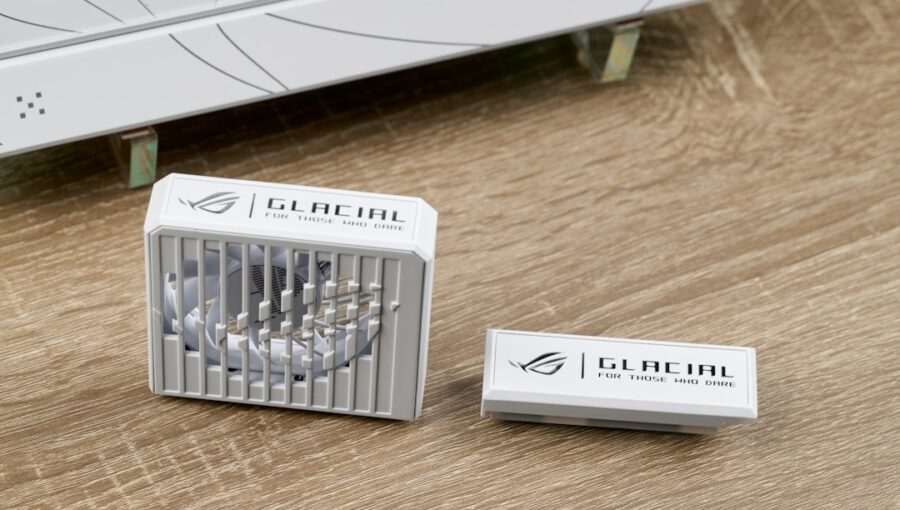
High-performance semiconductor packaging is facing a serious heat problem, and frankly, traditional cooling methods just aren’t cutting it anymore. We’re seeing ever-increasing power densities in chips, especially with AI accelerators, high-end CPUs, and advanced networking ASICs. This isn’t just about making things uncomfortable; excessive heat directly impacts performance, reliability, and ultimately, the lifespan of these expensive components. The quick answer to how we’re tackling this is through a multifaceted approach, combining advanced materials, innovative architectural designs for heat removal, and increasingly, integration of active cooling directly into or very close to the package itself. It’s a race to get heat away from where it’s generated, faster and more efficiently than ever before.
The Escalating Thermal Challenge in Modern Packaging
Let’s be clear: the thermal management game has fundamentally changed. For decades, engineers could often rely on bigger heat sinks, more powerful fans, or perhaps a heat pipe here and there. Those days are largely behind us for cutting-edge devices. The sheer density of transistors and the power consumed within a tiny footprint mean that heat flux – the amount of heat passing through a given area – has skyrocketed. We’re talking heat densities that can rival a nuclear reactor core or a rocket nozzle, albeit over a much smaller area.
Why Heat Is the Enemy
It’s not just about things getting hot. Heat degrades semiconductor performance. As temperatures rise, electron mobility decreases, leading to slower switching speeds and increased leakage current. This translates directly into reduced clock speeds or, conversely, increased power consumption to maintain performance. Then there’s reliability. High temperatures accelerate various degradation mechanisms, like electromigration, dielectric breakdown, and solder joint fatigue. This means your expensive chip dies sooner, leading to higher failure rates and shorter product lifespans. Nobody wants that. Finally, there’s the economic impact. If you can’t cool a chip effectively, you might have to underclock it or de-rate its performance, leaving potential computing power on the table. This is a significant concern in data centers, where every joule of energy and every clock cycle counts towards operational efficiency and return on investment.
The Power Density Conundrum
Consider modern chip architectures. We’re stacking dies (3D ICs), integrating heterogeneous components onto a single package (chiplets), and pushing transistor counts into the tens of billions. Each of these advancements brings immense computational power, but they also bring their own thermal baggage. When you stack chips, heat generated in a lower layer has to pass through the layers above it to escape, creating “hot spots” and complex thermal pathways. Chiplets, while offering manufacturing flexibility, introduce new interfaces and materials that might not be as thermally conductive as a monolithic die. It’s not just the total power, but how concentrated that power is, that defines the thermal challenge. This concentration is what we mean by power density, and it’s the primary driver pushing for these next-gen solutions.
In the realm of advanced semiconductor packaging, effective thermal management is crucial for enhancing performance and reliability. A related article that explores the importance of selecting the right devices for optimal performance in various environments can be found at Best Laptops for Kids 2023. This article highlights how appropriate thermal solutions can significantly impact the efficiency of high-performance electronics, making it a valuable read for those interested in the intersection of technology and thermal management.
Key Takeaways
- The training data includes information and events up to October 2023.
- Insights and knowledge are based on a wide range of sources available until the cutoff date.
- No updates or developments occurring after October 2023 are included in the training.
- Users should verify current information from reliable sources for the latest updates.
- The model’s responses reflect the context and knowledge available up to the specified date.
Advanced Materials for Thermal Dissipation

The first line of defense against heat is often material science. We’re constantly looking for materials that can either conduct heat away more effectively or spread it out more efficiently. This involves everything from the substrate itself to the thermal interface materials (TIMs) that bridge gaps between components.
High Thermal Conductivity Substrates
Traditional organic substrates, like those made from BT resin (Bismaleimide-Triazine), have served us well, but their thermal conductivity is relatively low. For high-power applications, we’re seeing a shift towards materials with much better heat transport properties. Silicon carbide (SiC) and aluminum nitride (AlN) ceramics are excellent examples. They offer significantly higher thermal conductivity and also have a good match in coefficient of thermal expansion (CTE) with silicon, which helps reduce thermomechanical stress during heating and cooling cycles. Even diamond, with its incredibly high thermal conductivity, is being explored, though its cost and manufacturing challenges remain significant hurdles for widespread adoption. Glass, too, is gaining traction, particularly for interposers in 2.5D and 3D packages. While glass itself isn’t a fantastic thermal conductor, its perfectly smooth surface and ability to support very fine interconnects make it attractive. The focus then shifts to how heat can be conducted through the glass, often via embedded microvias filled with highly conductive materials.
Enhanced Thermal Interface Materials (TIMs)
TIMs are critical. They fill the microscopic air gaps and imperfections between two surfaces (like a chip and a heat spreader), which are terrible thermal conductors. The goal for TIMs is not just high thermal conductivity but also low thermal resistance, good wettability, and long-term stability under thermal cycling. We’re moving beyond simple thermal greases and pads. Liquid metals, often gallium-indium alloys, offer superior thermal conductivity compared to traditional polymer-based greases. However, they can be corrosive to some metals (like aluminum) and are electrically conductive, requiring careful application. Phase-change materials (PCMs) are another option; they change from a solid to a liquid at a specific temperature, providing excellent surface conformance and a low thermal resistance during operation. Furthermore, research into advanced fillers for traditional TIMs is ongoing, incorporating materials like graphene, carbon nanotubes, and boron nitride nanoparticles to boost their thermal performance significantly. The challenge is ensuring these fillers don’t compromise other critical properties like bond line thickness or long-term reliability.
Novel Heat Spreading Layers
Spreading heat laterally before it’s dissipated into the ambient air or liquid is crucial. Vapor chambers, essentially flattened heat pipes, are becoming standard in high-end packages. They utilize a phase-change cycle (evaporation and condensation of a working fluid) to efficiently transfer heat over a larger area with very little temperature drop. Advanced vapor chambers are being developed with thinner profiles and more complex internal wick structures to handle even higher heat fluxes. Beyond conventional metals like copper, materials like pyrolytic graphite sheets (PGS) are also being used. PGS has anisotropic thermal conductivity, meaning it conducts heat exceptionally well along its plane but poorly perpendicular to it. This makes it ideal for spreading localized hot spots over a wider area without adding much thickness.
Architectural Innovations in Packaging

It’s not just about the materials; it’s about how we design the entire thermal pathway from the chip to the outside world. This involves rethinking how packages are constructed and how cooling mechanisms are integrated.
2.5D and 3D Packaging Thermal Challenges
When you move from 2D (chips side-by-side) to 2.5D (chips on an interposer) and 3D (chips stacked vertically), the thermal challenges multiply. In 2.5D, the interposer itself can become a thermal bottleneck if not designed properly. Heat from the logic die and high-bandwidth memory (HBM) stacks has to traverse the interposer.
This has led to concepts like thermally enhanced interposers, which might incorporate microchannels for liquid cooling or embedded high-conductivity pathways.
In 3D stacking, the problem becomes even more acute. Chips in the middle of a stack can get “sandwiched” thermally, with heat generated both above and below them. This often requires through-silicon vias (TSVs) to be designed not just for electrical connectivity but also with thermal considerations in mind.
Some advanced 3D concepts even explore “thermal TSVs” that are specifically designed to conduct heat and not electricity, or even liquid-filled microchannels directly within the stacked dies. The goal is to provide a direct, low-resistance thermal path for each die in the stack, rather than relying on heat to propagate through multiple layers.
Integrated Heat Sinks and Microfluidics
The traditional approach of attaching a large heat sink to the top of a package is becoming insufficient. We’re seeing a trend towards integrating cooling closer to the heat source.
This could mean embedding microfluidic channels directly into the package substrate or even into the back of the silicon die itself. These microchannels circulate a dielectric coolant, removing heat very efficiently through direct contact with the chip. This “liquid cooling at the chip level” significantly reduces the thermal resistance between the heat source and the cooling medium.
Another approach is to create highly effective, miniature heat sinks as part of the package itself.
This might involve complex fin structures manufactured directly on the package or even in the silicon lid, providing more surface area for heat exchange within a very confined space. The challenge here is manufacturing precision and ensuring reliable sealing for any liquid-based solutions.
Cold Plates and Advanced Manifolds
For server-level applications, sophisticated cold plates are essential. These are not just flat blocks of metal; they incorporate intricate internal geometries, like micro-fins or jet impingement nozzles, to maximize heat transfer to a circulating liquid coolant.
The design of these cold plates is highly optimized using computational fluid dynamics (CFD) to ensure uniform flow and efficient heat extraction across the entire surface of the processor. Furthermore, the manifolding systems that deliver and remove the coolant to these cold plates are becoming increasingly complex, designed to minimize pressure drop and ensure consistent flow rates to multiple packages in a dense rack environment. Quick-disconnect fittings and leak detection systems are also critical components of these advanced liquid cooling infrastructures.
Active Cooling Approaches
While passive thermal management (materials and design) is crucial, some high-power applications are pushing us towards active cooling solutions that require external power input.
Direct-to-Chip Liquid Cooling
This is arguably one of the most promising avenues for extremely high-power packages. Instead of a traditional heat spreader and external heat sink, a cold plate is mounted directly onto the bare die, or even integrated into the package lid.
A dielectric fluid (one that doesn’t conduct electricity) is pumped through microchannels in this cold plate, absorbing heat directly from the chip’s surface.
This method can remove significantly more heat than air cooling because liquids have a much higher specific heat capacity and thermal conductivity than air.
There are two main categories: single-phase and two-phase liquid cooling. In single-phase, the fluid remains liquid throughout the cooling cycle, simply absorbing heat and carrying it away. In two-phase cooling, the fluid boils and vaporizes as it absorbs heat, then condenses back to a liquid in a remote heat exchanger. This phase change process is extremely efficient at transferring large amounts of heat with very little temperature difference. The challenges with direct-to-chip liquid cooling include managing leaks, ensuring compatibility of materials with the dielectric fluid, and integrating the pumping and heat rejection systems into the overall platform.
Thermoelectric Coolers (TECs)
TECs, also known as Peltier devices, utilize the Peltier effect to create a temperature difference across their junctions when an electrical current is applied. One side gets cold, and the other gets hot. They are essentially solid-state heat pumps. TECs are particularly useful for creating localized cooling, allowing specific hot spots on a chip to be actively cooled below the ambient temperature or the temperature of the main cooling system. This “spot cooling” can be crucial for optimizing performance in areas of a chip that generate disproportionately more heat.
However, TECs have their own challenges. They consume electrical power to operate, and their efficiency (coefficient of performance) isn’t always high, meaning they generate additional heat that then needs to be removed by the primary cooling system. They also have a maximum heat pumping capacity and a limited temperature differential they can achieve. Despite these drawbacks, ongoing research into more efficient thermoelectric materials and novel TEC designs continues to make them a viable option for specialized, targeted cooling applications where precise temperature control is paramount.
Immersion Cooling
Taking liquid cooling to the extreme, immersion cooling involves submerging entire server racks or individual components directly into a dielectric fluid. This can be single-phase (fluid remains liquid) or two-phase (fluid boils and condenses). In single-phase immersion, the fluid circulates and is cooled by a heat exchanger. In two-phase, the fluid boils directly on the chip surfaces, and the vapor rises to a condenser at the top of the tank, where it cools and drips back down.
Immersion cooling offers exceptional thermal management capabilities, as every surface of every component is in direct contact with the coolant. This eliminates the need for fans, heat sinks, and even TIMs in many cases, leading to a quieter, more power-efficient, and potentially more compact system. It also provides excellent temperature uniformity across components. The hurdles include the cost of the dielectric fluids, infrastructure changes required for data centers, fluid compatibility with various materials, and maintenance procedures. Despite these, it’s gaining significant traction in hyperscale data centers and supercomputing environments where power density is paramount.
In the realm of advanced semiconductor packaging, effective thermal management is crucial for enhancing performance and reliability. A related article discusses innovative solutions that can significantly improve thermal efficiency in high-performance applications. For those interested in exploring more about this topic, you can read about the best free software for translation, which may also provide insights into optimizing processes in various engineering fields. Check it out here.
Modeling and Simulation Tools
| Metric | Value | Unit | Description |
|---|---|---|---|
| Thermal Conductivity of TIM | 15 | W/m·K | Thermal Interface Material conductivity for efficient heat transfer |
| Maximum Junction Temperature | 125 | °C | Maximum allowable temperature for semiconductor junction |
| Heat Flux Density | 500 | W/cm² | Heat dissipation rate per unit area in high-performance chips |
| Thermal Resistance (Package to Ambient) | 0.5 | °C/W | Resistance to heat flow from semiconductor package to environment |
| Cooling Efficiency Improvement | 30 | % | Improvement in cooling performance using next-gen thermal solutions |
| Operating Power Density | 100 | W/cm² | Power dissipation per unit area in high-performance semiconductor devices |
| Thermal Cycling Reliability | 1000 | Cycles | Number of thermal cycles the packaging can withstand without failure |
Designing effective next-gen thermal management systems isn’t a trial-and-error process anymore. It relies heavily on sophisticated computational tools to predict thermal behavior before anything is even built.
Computational Fluid Dynamics (CFD)
CFD is indispensable for analyzing fluid flow and heat transfer. For thermal management, CFD models are used to simulate the movement of air or liquid coolants, predict temperature distributions, and identify potential hot spots within a package, a cold plate, or an entire server rack. Engineers can use CFD to optimize fin designs in heat sinks, analyze flow paths in microchannels, and predict pressure drops across complex cooling structures. This allows for virtual prototyping and optimization, significantly reducing the number of physical prototypes needed and accelerating design cycles. Modern CFD tools can handle incredibly complex geometries and transient thermal events, providing detailed insights into how a system will behave under various operating conditions.
Finite Element Analysis (FEA)
While CFD focuses on fluid dynamics, FEA is primarily used for structural and thermal stress analysis within solid materials. In semiconductor packaging, FEA is crucial for understanding how different materials with varying coefficients of thermal expansion (CTE) behave under temperature changes. For example, it can predict warpage in substrates, stress on solder joints, or delamination risks in multi-layered packages due to thermal cycling. By integrating FEA with thermal simulations, engineers can ensure that a proposed cooling solution doesn’t introduce new mechanical reliability issues. This is especially important for heterogeneous integration and 3D stacking, where complex material interfaces are prevalent.
Multiphysics Simulation
The reality of thermal management in advanced packaging is that it’s rarely just a thermal problem. It’s a multiphysics problem. Heat generation is influenced by electrical behavior (power dissipation), and temperature, in turn, affects electrical performance. Mechanical stresses arising from thermal expansion can lead to failures. Therefore, multiphysics simulation tools, which can simultaneously model electrical, thermal, and mechanical phenomena, are becoming essential. These tools allow engineers to observe how changes in one domain (e.g., increased current) impact others (e.g., temperature rise and subsequent mechanical stress). This integrated approach provides a much more holistic and accurate understanding of package behavior, enabling more robust and reliable designs from the outset.
Future Trends and Outlook
The quest for better thermal management is an ongoing race, and several exciting areas are still under active development.
Thermal-Aware Design Automation
As chips become more complex, manual thermal design is increasingly impractical. The future will involve more thermal-aware design automation tools that integrate thermal considerations directly into the electronic design automation (EDA) flow. This means that architects and designers will get real-time feedback on the thermal implications of their choices, from transistor layout to package assembly. Tools will be able to suggest optimal placement of components, routing of power, and even dynamic power management strategies based on predicted thermal profiles. This proactive approach aims to “design out” thermal problems before they become critical.
Advanced Nano-scale Thermal Engineering
At the very smallest scales, new physics comes into play. Research into nano-scale thermal engineering is exploring novel ways to manipulate heat at the atomic level. This includes using superlattices, phonon engineering, and materials with tailored phonon scattering properties to direct heat flow or create thermal rectifiers. While still largely in the research phase, these breakthroughs could lead to ultra-thin thermal insulation, highly efficient heat pipes, or even on-chip thermoelectric devices with unprecedented performance. The ability to control heat at this fundamental level could unlock entirely new thermal management paradigms.
Hybrid Cooling Solutions
It’s unlikely that a single cooling solution will dominate for all applications. Instead, we’ll see a rise in sophisticated hybrid cooling solutions. This might involve combining microfluidics for direct-to-chip cooling, with vapor chambers for lateral heat spreading, and perhaps a small TEC for localized hot spot removal, all within a single package or system. The integration of these different techniques will require careful design and optimization to ensure they work seamlessly together, leveraging the strengths of each method to achieve optimal thermal performance and power efficiency. This complexity demands even more sophisticated modeling and integration capabilities.
Sustainable Thermal Management
Finally, there’s a growing focus on sustainability. Data centers consume vast amounts of energy, and a significant portion goes to cooling.
Future thermal management solutions will not only aim for performance but also for energy efficiency and environmental friendliness.
This means exploring refrigerants with lower global warming potential, developing closed-loop liquid cooling systems that minimize water consumption, and even looking into waste heat recovery technologies that capture and reuse the heat generated by electronics. The goal is to make high-performance computing not just powerful, but also greener and more resource-efficient. This holistic view of thermal management extends beyond the package itself to the entire ecosystem it operates within.
FAQs
What is thermal management in semiconductor packaging?
Thermal management in semiconductor packaging refers to the techniques and technologies used to control and dissipate heat generated by high-performance semiconductor devices to ensure optimal operating conditions and prevent overheating.
Why is thermal management important in high-performance semiconductor packaging?
Thermal management is crucial in high-performance semiconductor packaging to maintain the reliability, efficiency, and longevity of the semiconductor devices. Excessive heat can lead to performance degradation, premature failure, and reduced overall system performance.
What are some next-gen thermal management solutions for high-performance semiconductor packaging?
Next-gen thermal management solutions for high-performance semiconductor packaging include advanced materials such as thermal interface materials (TIMs), heat spreaders, heat sinks, vapor chambers, and microfluidic cooling technologies. These solutions help improve heat dissipation and thermal conductivity in semiconductor packages.
How do next-gen thermal management solutions benefit high-performance semiconductor packaging?
Next-gen thermal management solutions offer improved heat dissipation capabilities, enhanced thermal conductivity, reduced thermal resistance, and better thermal stability. These benefits help optimize the performance, reliability, and efficiency of high-performance semiconductor devices.
What are the challenges in implementing next-gen thermal management for high-performance semiconductor packaging?
Challenges in implementing next-gen thermal management solutions for high-performance semiconductor packaging include cost considerations, compatibility with existing packaging technologies, integration complexity, and the need for advanced manufacturing processes. Addressing these challenges is essential to fully leverage the benefits of next-gen thermal management solutions.
Enjoying our content? Make us a preferred source on Google:
Add us as a Preferred Source on Google