

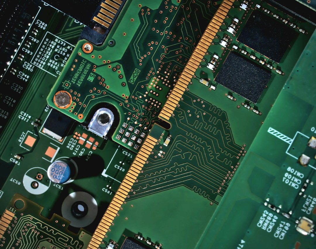
So, you’re probably wondering if biodegradable printed circuit boards (PCBs) are a real thing and if they can actually help with our massive electronic waste problem. The short answer is yes, they are a developing reality, and they hold significant promise as one crucial tool in the fight against the ever-growing mountain of discarded electronics. While not a silver bullet, these innovative boards offer a path toward more sustainable electronics manufacturing and consumption by designing for end-of-life degradation rather than perpetual landfilling. Let’s dig into what they are, why they matter, and the exciting progress being made.
The Mounting Pressure of Electronic Waste
It’s no secret that we’re generating an alarming amount of electronic waste, or e-waste, every year. Think about it: how many old phones, laptops, and various gadgets do you have tucked away in drawers, or worse, have you thrown out? This isn’t just an unsightly problem; it’s a deeply concerning environmental and health crisis.
The Scale of the Problem
Globally, we produce tens of millions of metric tons of e-waste annually. To put that into perspective, imagine a line of fully loaded 40-ton articulated trucks stretching from New York City to Bangkok – that’s roughly the amount of e-waste we’re talking about in a single year. And this number is only expected to grow as technology advances and consumer appetites for new devices remain high. Much of this waste ends up in landfills, where it can sit for centuries, slowly leaching harmful substances into the soil and groundwater.
Hazardous Materials in Traditional PCBs
One of the biggest culprits in e-waste is the conventional printed circuit board itself. These boards are the backbone of virtually all electronic devices, but they’re typically made from non-biodegradable materials like fiberglass (FR-4 laminate) and epoxy resins. What’s more concerning are the various heavy metals and flame retardants embedded within them. Lead, mercury, cadmium, and brominated flame retardants (BFRs) are just a few examples. When these materials break down or are improperly processed, they can release toxic chemicals into the environment, posing serious health risks to both people and wildlife. Traditional recycling of these complex composites is also energy-intensive and often only recovers a fraction of the valuable materials, leaving behind a problematic residue.
Limited Recycling Effectiveness
While recycling programs exist, the reality is that a significant portion of e-waste isn’t properly recycled. There are many reasons for this: lack of awareness, difficulty of collection, the complex mix of materials in devices, and economic viability. Even when devices are recycled, the process for PCBs is often challenging. Separating the various layers – copper traces, polymer substrates, and solder – is difficult and costly. This leads to a situation where valuable resources are lost, and hazardous components continue to pollute. This is where biodegradable PCBs offer a compelling alternative.
In the quest for sustainable technology, the development of biodegradable printed circuit boards (PCBs) is a significant advancement in addressing the escalating crisis of electronic waste. As industries increasingly turn to eco-friendly solutions, understanding the broader implications of sustainability in various sectors becomes essential. A related article that explores the intersection of sustainability and business practices is available at Top Trends in E-Commerce Business, which discusses how e-commerce companies are adapting to consumer demands for environmentally responsible products and practices. This highlights the growing importance of integrating sustainable innovations like biodegradable PCBs into the fabric of modern technology and commerce.
Key Takeaways
- The training data includes information and events up to October 2023.
- Insights and knowledge are based on a wide range of sources available until the cutoff date.
- No updates or developments occurring after October 2023 are included in the training.
- Users should verify current information from reliable sources for the latest updates.
- The model’s responses reflect the context and knowledge available up to the specified date.
Understanding Biodegradable PCB Technology
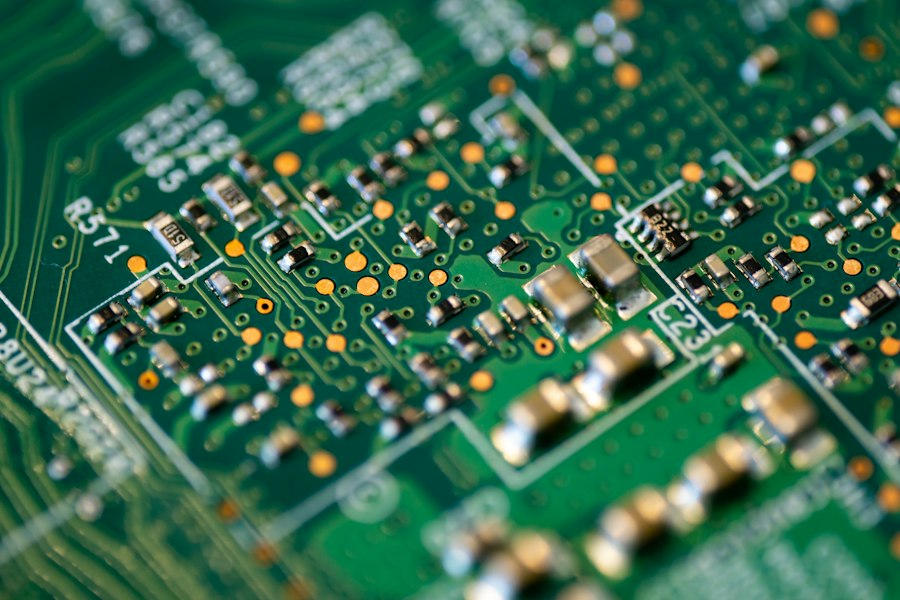
So, what exactly makes a PCB “biodegradable”? It comes down to the materials used in its construction. Instead of relying on conventional plastics and resins that persist for millennia, these innovative boards incorporate materials that can naturally break down into benign components under specific environmental conditions, like composting or microbial action.
Substrate Materials
The substrate is the foundational layer of the PCB, traditionally made from FR-4. For biodegradable PCBs, researchers are exploring and developing a range of alternative materials. These include various biopolymers derived from natural sources. Cellulose-based materials, often sourced from wood pulp or even agricultural waste, are particularly promising due to their abundance, low cost, and good mechanical properties. Starch-based polymers, polylactic acid (PLA) derived from corn starch or sugarcane, and even lignin (a complex polymer found in plant cell walls) are also being investigated. These materials can be engineered to possess similar dielectric properties and mechanical strength to traditional substrates, making them suitable for electronic applications. The key is that, unlike fiberglass, these materials can decompose at the end of their life cycle.
Conductive Inks and Traces
Beyond the substrate, the conductive pathways (traces) are another critical component. Traditional PCBs use copper, which is recyclable but requires energy-intensive processes to recover.
Biodegradable PCBs are exploring alternatives for their conductive elements.
Silver nanoparticles embedded in biodegradable polymers, conductive polymers like PEDOT:PSS, and even carbon-based inks are being developed. The goal is to create conductive materials that can either degrade along with the substrate or be easily separated and recovered in a more environmentally friendly manner. While copper is still a robust choice for performance, the focus on its end-of-life separation or integration into a degradable matrix is paramount. Some approaches even involve creating ultra-thin, easily detachable copper layers.
Interconnects and Components
The challenge extends to the interconnects and the components themselves. Biodegradable solder, often utilizing bismuth or tin alloys with lower melting points and less toxicity than lead-based solders, is an active area of research. Attaching traditional, non-biodegradable components (like integrated circuits, resistors, and capacitors) to a biodegradable board presents a conundrum. One strategy is to design the board for easy disassembly, allowing for the salvage of valuable or hazardous components while the substrate degrades. Another innovative approach involves the development of entirely biodegradable components, though this is a much more complex and long-term goal. For instance, creating fully biodegradable capacitors or transistors is a frontier still largely being explored.
Advantages and Challenges of Biodegradable PCBs
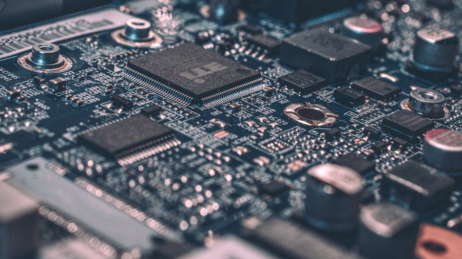
While the concept of biodegradable PCBs is undeniably appealing, it’s important to have a balanced view, understanding both the significant benefits they offer and the hurdles that need to be overcome before widespread adoption.
Environmental Benefits
The most obvious and compelling advantage is the drastic reduction in e-waste going to landfills. When a device with a biodegradable PCB reaches its end-of-life, the board can be composted or degraded, returning its constituent materials to the earth in a harmless form. This not only prevents the accumulation of waste but also mitigates the leaching of toxic chemicals associated with traditional PCBs. It also reduces the demand for virgin resources, as some biodegradable materials are derived from renewable sources. Furthermore, the energy required for complex recycling processes for traditional PCBs could be reduced, as the focus shifts to simpler degradation pathways.
This is a significant step towards a circular economy where materials are reused or naturally reintegrated rather than discarded.
Technical Challenges
Despite the promise, there are significant technical hurdles. Performance parity is a major concern. Biodegradable materials often have different electrical and thermal properties compared to conventional FR-4.
Maintaining signal integrity, managing heat dissipation, and ensuring durability over the product’s lifespan are critical. For instance, some bioplastics can be more susceptible to moisture or have lower heat deflection temperatures, which is problematic for components that generate heat. The mechanical strength and rigidity must also be sufficient to support components and withstand assembly processes.
Achieving reliable conductive traces with biodegradable materials that can handle the necessary current and frequency requirements without compromising performance is another area of intense research. Miniaturization, a constant drive in electronics, also adds complexity to using alternative materials.
Economic and Scalability Challenges
The cost of manufacturing biodegradable PCBs is currently higher than traditional boards due to smaller production volumes, specialized materials, and less mature manufacturing processes. For widespread adoption, these costs need to become competitive.
Supply chain development is another factor; ensuring a consistent, high-quality supply of suitable biodegradable materials at scale is crucial. Furthermore, the existing infrastructure for PCB manufacturing is heavily invested in FR-4 technology. Shifting to new materials and processes requires significant capital investment and retraining.
Consumer acceptance also plays a role; while environmentally conscious consumers might be willing to pay a premium, mainstream adoption often hinges on comparable pricing and performance.
Current Research and Development Pathways
The field of biodegradable PCBs is rapidly evolving, with researchers and companies exploring a diverse array of materials and manufacturing techniques to bring these sustainable solutions to fruition.
Novel Material Synthesis
A significant portion of current research focuses on synthesizing and characterizing new biodegradable polymers that can meet the stringent requirements of electronics. Scientists are experimenting with various natural fibers – like bamboo, silk, and even paper – as reinforcement materials for bioplastic matrices. The goal is to create composites that offer the necessary mechanical strength, thermal stability, and dielectric properties. For instance, modified cellulose papers coated with biodegradable resins are showing promise as flexible and degradable substrates. Another exciting area involves developing self-healing biodegradable polymers, which could extend the lifespan of devices and reduce early e-waste. Efforts are also underway to create bio-based epoxies and resins that can serve as binding agents, replacing petroleum-derived alternatives.
Additive Manufacturing and Printing Techniques
Additive manufacturing, such as 3D printing and inkjet printing, is proving to be a game-changer for biodegradable PCBs. These techniques allow for the precise deposition of conductive inks and biodegradable polymer layers, reducing material waste and enabling complex, customized designs. Imagine printing a circuit board directly from a digital file, using only the necessary amount of material. This approach is particularly well-suited for prototypes and small-batch production, and as the technology matures, it could become viable for larger scales. Inkjet printing of conductive silver nanoparticle inks onto flexible biopolymer substrates is an example of this, allowing for circuit patterns to be formed without traditional etching processes that consume harsh chemicals. This also opens possibilities for integrating sensors and other functionalities directly into the substrate.
Hybrid Approaches and Modular Design
Recognizing the difficulty of making every single component biodegradable, many researchers are pursuing hybrid approaches. This involves designing PCBs where the substrate is biodegradable, but critical, non-biodegradable components are easily removable and recyclable. Think of it as a modular design philosophy where different parts of an electronic device are designed for different end-of-life pathways. For example, a phone could have a biodegradable main board, but the processor and memory chips would be designed to be easily popped out for reuse or high-value recycling. This strategy aims to maximize the benefits of degradable materials while still ensuring that valuable or problematic components are handled responsibly. This pragmatic approach could accelerate the adoption of biodegradable elements by not requiring a complete overhaul of component manufacturing.
In the ongoing discussion about sustainable technology solutions, the development of biodegradable printed circuit boards represents a significant advancement in addressing the escalating crisis of electronic waste. As consumers increasingly rely on electronic devices, the environmental impact of discarded gadgets becomes more pressing. A related article explores the competition between major smartwatch brands, highlighting how companies like Apple and Samsung are also considering eco-friendly practices in their product designs. For more insights on this topic, you can read about it in this comparison of the Apple Watch and Samsung Galaxy Watch.
The Future Landscape of Sustainable Electronics
| Metric | Value | Unit | Notes |
|---|---|---|---|
| Global E-Waste Generated (2023) | 57.4 | Million Metric Tons | According to Global E-Waste Monitor 2023 |
| Recycling Rate of E-Waste | 17.4 | Percent | Only a small fraction is properly recycled |
| Average PCB Composition | 30-40 | Percent | Percentage of total electronic device weight |
| Biodegradable PCB Decomposition Time | 6-12 | Months | Under industrial composting conditions |
| Traditional PCB Decomposition Time | 500+ | Years | Estimated time for natural degradation |
| Reduction in Toxic Waste Using Biodegradable PCBs | 70 | Percent | Compared to conventional PCBs |
| Cost Increase for Biodegradable PCBs | 10-15 | Percent | Compared to traditional PCBs |
| Projected Market Growth for Biodegradable PCBs | 18 | Percent CAGR | 2024-2030 forecast |
The journey toward widespread adoption of biodegradable PCBs is complex, but the trajectory is clear: electronics need to become more sustainable. Biodegradable PCBs are poised to play a pivotal role in this transformation, but they won’t be the sole solution.
Integration with Broader Sustainability Goals
Biodegradable PCBs are best viewed as one critical piece of a larger puzzle in creating a truly circular economy for electronics. This future involves a holistic approach that includes: designing products for longevity and repairability, promoting robust take-back and recycling schemes, developing efficient material recovery technologies, and fostering responsible consumption patterns. The environmental impact of manufacturing the components themselves, even if they are placed on a biodegradable board, also needs to be considered. Ultimately, the goal is to minimize resource extraction and waste generation throughout the entire lifecycle of an electronic device, from raw material sourcing to end-of-life disposal.
Policy and Industry Drivers
For biodegradable PCBs to move from niche applications to mainstream, strong policy support and industry commitment will be essential. Governments can incentivize research and development, establish standards for biodegradability and compostability, and create regulations that mandate higher levels of sustainable materials in electronics. Extended Producer Responsibility (EPR) schemes, which hold manufacturers accountable for the entire lifecycle of their products, could be expanded to specifically encourage the use of biodegradable components. Industry leaders, through collaborative initiatives and investments in green technologies, can drive down costs and scale up production. Consumer demand for more sustainable products will also exert pressure on manufacturers to adopt these technologies.
The Road Ahead
While fully biodegradable devices are likely still some time away, the incremental adoption of biodegradable PCBs in less demanding applications, such as disposable medical sensors, smart packaging, or low-cost IoT devices, is already happening. As materials improve and manufacturing processes become more efficient, we can expect to see them integrated into more complex electronics. Continuous research into advanced materials, improved manufacturing techniques, and effective end-of-life processing solutions will be key. The collaboration between material scientists, electronics engineers, and policymakers will be crucial in overcoming the remaining challenges and ushering in an era where electronic waste is no longer an escalating crisis, but a manageable part of a sustainable technological ecosystem. The prospect of an electronic device that can simply return to nature, leaving no harmful trace, is a powerful vision driving this vital innovation.
FAQs
What are biodegradable printed circuit boards (PCBs)?
Biodegradable printed circuit boards are electronic components designed to decompose naturally over time, reducing the environmental impact associated with traditional PCBs, which are typically made from non-biodegradable materials. These eco-friendly alternatives are often made from organic materials that can break down in natural environments, helping to mitigate electronic waste.
How do biodegradable PCBs help reduce electronic waste?
Biodegradable PCBs contribute to reducing electronic waste by providing a sustainable option for electronic components that can decompose after their useful life. This helps to minimize the accumulation of non-biodegradable materials in landfills and reduces the environmental hazards associated with traditional electronic waste disposal.
What materials are commonly used in biodegradable PCBs?
Common materials used in biodegradable PCBs include natural polymers such as cellulose, starch, and polylactic acid (PLA). These materials are chosen for their ability to break down in the environment while still providing the necessary electrical and mechanical properties required for electronic applications.
Are biodegradable PCBs as effective as traditional PCBs?
While biodegradable PCBs are still being developed and optimized, many current prototypes demonstrate comparable performance to traditional PCBs in terms of electrical conductivity and durability. However, ongoing research aims to enhance their reliability and lifespan to meet the demands of various electronic applications.
What challenges are associated with the adoption of biodegradable PCBs?
Challenges in adopting biodegradable PCBs include the need for improved manufacturing processes, ensuring compatibility with existing electronic components, and addressing concerns about performance and longevity. Additionally, there is a need for industry standards and regulations to facilitate widespread acceptance and integration into the electronics market.
Enjoying our content? Make us a preferred source on Google:
Add us as a Preferred Source on Google